Loading Port:Shanghai Port
Payment Terms:TT or LC
Min Order Qty:100 Pieces PCS
Supply Capability:700MW/Per Year PCS/month
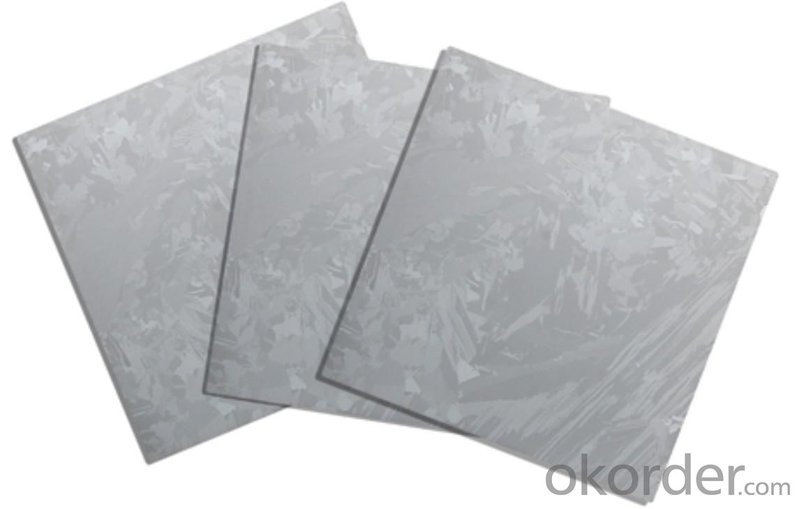
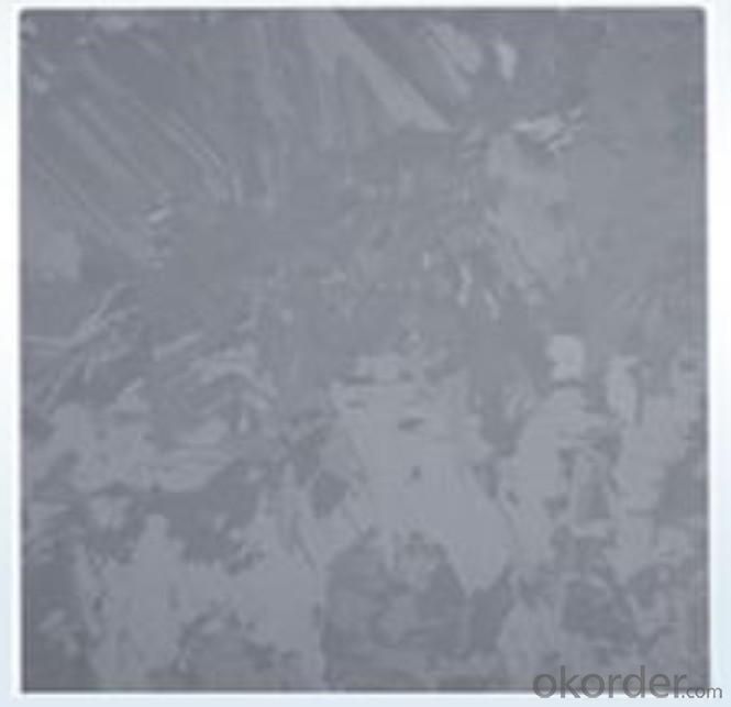
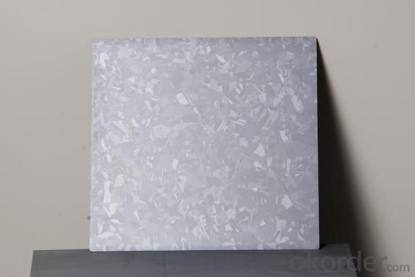
Specifications of Polycrystalline Silicon Wafer
Format : 156 mm × 156 mm ± 0.5 mm
Thickness : 200μm ± 10 μm
| Product name | Poly Wafer |
| Conductive type | P Type |
| Square size wafer (mm) | 156×156±0.5 |
| 219.20±0.5 | |
| Corner (mm)
|
1±0.5、45°±10º |
| 200±20 | |
| Total thickness(um) | ≤40 |
| Resistivity ranges(Ωcm) | 1-3 |
| Doping elements | boron |
| Carbon content(atoms/cc) | ≤8*1017 |
| Oxygen content(atoms/cc) | ≤1*1018 |
| Lifetime(μs) | ≥2 |
| Surface quality | No crack, gap, missing Angle, perforated, window, microcrystalline |
| Warping degrees(μm) | ≤50 |
| Neighbouring vertical degree | 90±0.5° |
| Side damage(mm) | ≤0.5mm(length)×0.3mm(width),(not more than 2 per wafer) |
| Line mark(μm) | ≤15 |
Usage and Applications of Poly Wafers
Poly Solar Wafers mainly used in Poly Solar Cells, with high efficiency and reliable quality. Our Wafer can promise the 25 years life span and have passed PID test.
Packaging & Delivery of Poly Wafers
Carton Box Package and Deliver by air
Factory Picture of Poly Wafers

Package Picture of Poly Wafers