Loading Port:China Main Port
Payment Terms:TT or LC
Min Order Qty:100 Pcs PCS
Supply Capability:700 MW/Per Year PCS/month
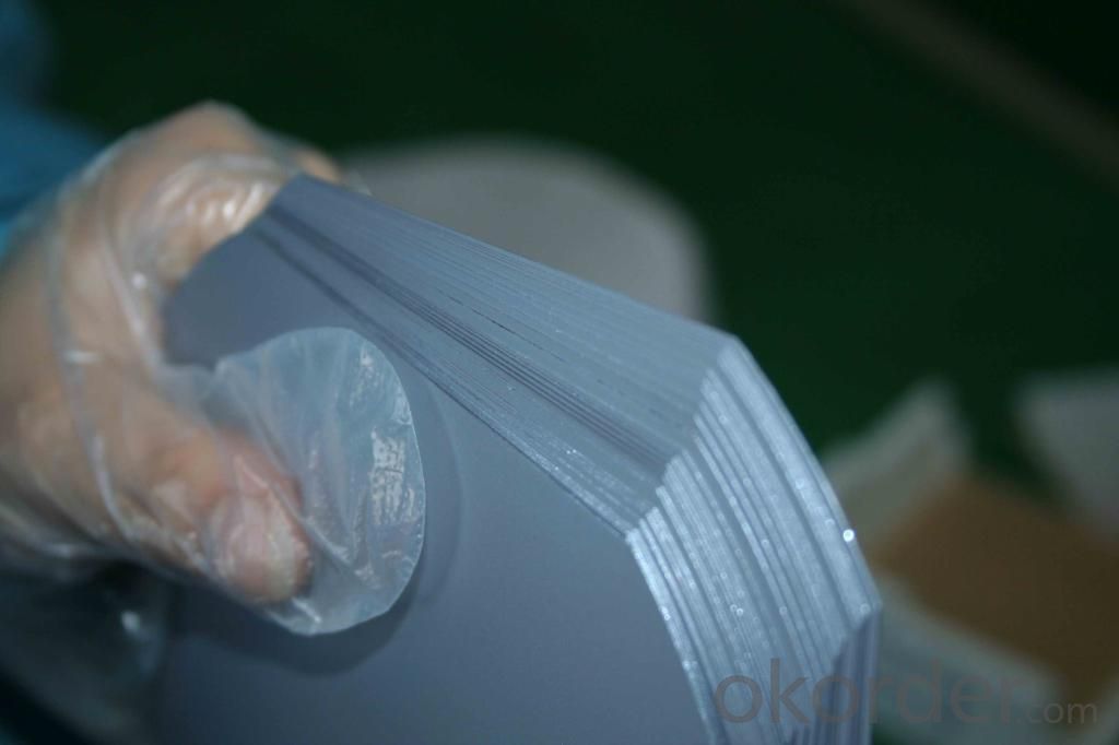
Specification of Mono Silicon Wafer
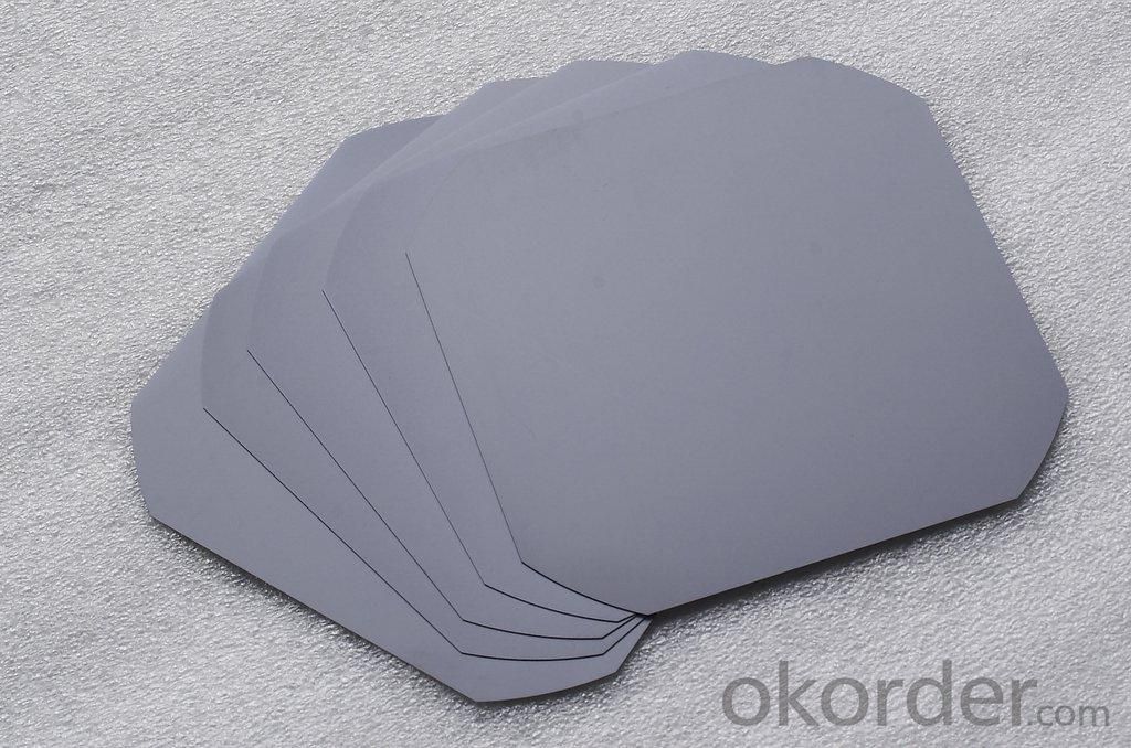
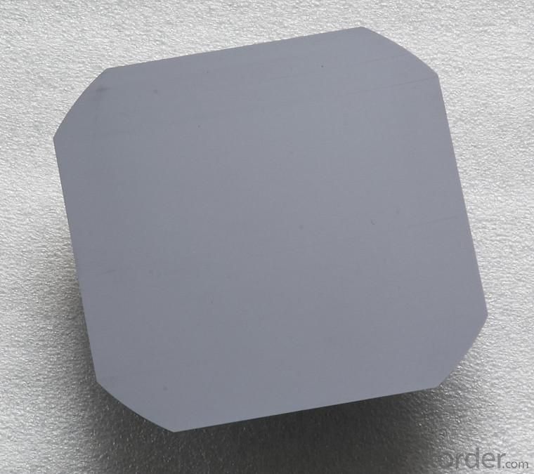
We can provide you solar wafer 156*156mm Mono Wafers for your raw materials choice.
| Product name | Mono Wafer |
| Conductive type | P type |
| Square size wafer(mm) | 156×156±0.5 |
| Resistivity | 1~3 ohm |
| Corner(mm) | 150±0.5;165±0.5 |
| 195±0.5;200±0.5 | |
| Thickness (μm) | 200±20 |
| Total thickness(um) | ≤ 30 |
| Resistivity range(Ωcm) | 1-3 |
| Doping elements | Boron |
| Orientation | (100)±1° |
| Carbon content(atoms/cc) | ≤1.0E+17 |
| Oxygen content(atoms/cc) | ≤1.0E+18 |
| Lifetime(μs) | ≥10 |
| Surface quality | No crack, gap, missing Angle, perforated, silicon fell and stress |
| Warping degrees(warp/μm) | ≤50 |
| Neighbouring vertical degree | 90±0.5° |
| Side damage(mm) | ≤0.5mm(length)×0.3mm(width)(not more than 2 per wafer) |
| Line mark(μm) | ≤15 |
Usage and Applications of Mono Wafers
Mono Solar Wafer mainly used in Mono Solar Cells with reliable quality and trustful efficiency performance. Our Mono Wafers should be your best choice for raw materials.
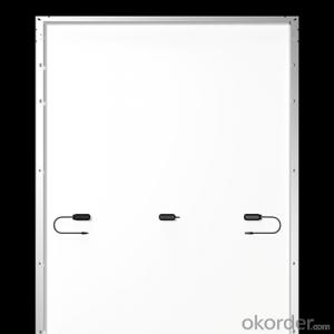
Packaging & Delivery of Mono Wafers
Carton Box Package and Deliver by air. Mono Wafers should be avoid of sunshine, moist, and water.
Factory Picture of Mono Wafers

Package Picture of Mono Wafers