Loading Port:Shanghai Port
Payment Terms:TT or LC
Min Order Qty:100 Pieces PCS
Supply Capability:700MW/Per Year PCS/month
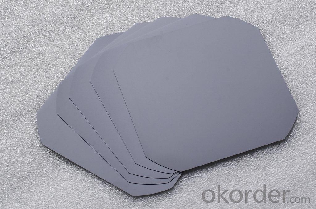
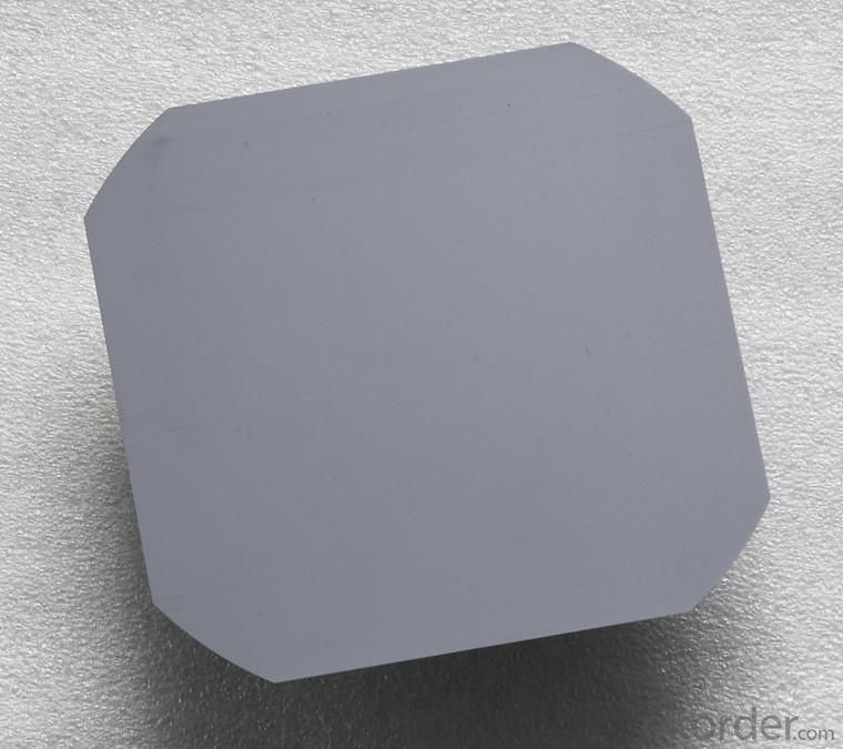
Monocrystalline solar wafer 125*125mm
Conductivity Type: P type
Dopant: Boron
Resistivity: 1~3 ohm
thickness: 200um.
| Product name | Mono Wafer |
| Conductive type | P type |
| Square size wafer(mm) | 125×125±0.5 mm |
| Resistivity | 1~3 ohm |
| Corner(mm) | 150±0.5;165±0.5 |
| 195±0.5;200±0.5 | |
| Thickness (μm) | 200±20 |
| Total thickness(um) | ≤ 30 |
| Resistivity range(Ωcm) | 1-3 |
| Doping elements | Boron |
| Orientation | (100)±1° |
| Carbon content(atoms/cc) | ≤1.0E+17 |
| Oxygen content(atoms/cc) | ≤1.0E+18 |
| Lifetime(μs) | ≥10 |
| Surface quality | No crack, gap, missing Angle, perforated, silicon fell and stress |
| Warping degrees(warp/μm) | ≤50 |
| Neighbouring vertical degree | 90±0.5° |
| Side damage(mm) | ≤0.5mm(length)×0.3mm(width)(not more than 2 per wafer) |
| Line mark(μm) | ≤15 |
Advantages of Mono Solar Wafers
1. High efficiency and High power.2. Long-term electrical stability.
3. Lowest price and Fastest delivery.
4. Good quality and good service.
5. Bulk supply
6. Good Warranty
7. Big Sale
8. More than 25 years on the lifetime.
Usage and Applications of Mono Solar Wafers
Mono Solar wafers is used to make Solar Cells. With high quality and stable quality. Our Solar Wafers can greatly improve the performance of Solar Cells.
Packaging & Delivery of Mono Solar Wafers
Carton Box Package and Deliver by air.It should be noticed that it should be avoid of water, sunshine and moist.
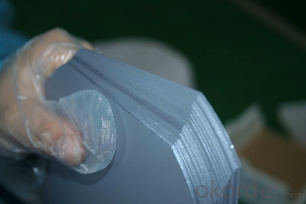
Wafer Factory Picture of Mono Solar Wafers

Package Picture of Mono Solar Wafers