Loading Port:China main port
Payment Terms:TT or LC
Min Order Qty:100000 pc
Supply Capability:1000000 pc/month
1. Structure of Monocrystalline Silicon Solar Wafer 125*125mm Description
A wafer, also called a slice or substrate, is a thin slice of semiconductor material, such as a crystalline silicon, used in electronics for the
fabrication of integrated circuits and in photovoltaics for conventional, wafer-based solar cells. The wafer serves as the substrate for
microelectronic devices built in and over the wafer and undergoes many microfabrication process steps such as doping or ion implantation,
etching, deposition of various materials, and photolithographic patterning. Finally the individual microcircuits are separated (dicing) and
packaged.
2. Main Features of the Monocrystalline Silicon Solar Wafer 125*125mm
• monocrystalline solar wafer 125*125mm
•Conductivity Type: P type
•Dopant: Boron
•Resistivity: 1~3 ohm
•thickness: 200um.
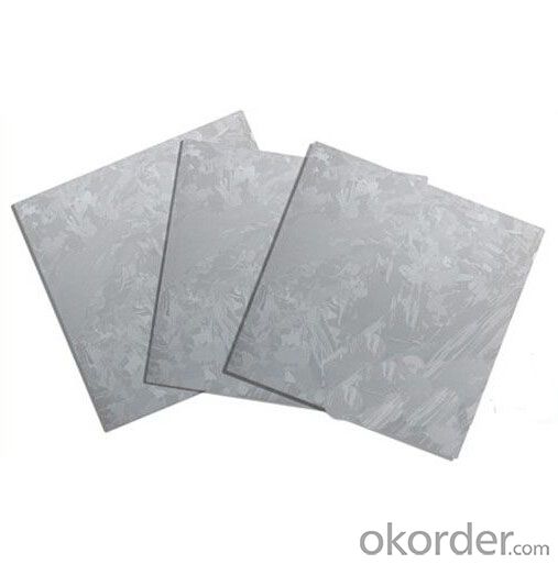
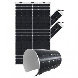
3. Monocrystalline Silicon Solar Wafer 125*125mm Images


4. Monocrystalline Silicon Solar Wafer 125*125mm Specification
Type: | P |
Dopant: | Boron |
Resistivity: | 1.0-3(ohmNaN) |
Dimension: | 125 x 125±0.5 (mm) |
Thickness: | 200±20 (μm) |
Oxygen Content: | ≤1 x 10¹⁸ |
Carbon Content: | ≤5x 10¹⁶ |
Minority Carrier Lifetime: | ≥2 (us) |
Microcrystal: | 10/cm2 |
Saw Depth: | <20 (μm) |
TTV: | <=30(μm)< span=""> |
Bow: | 50 (μm) |
Bevel Edge Angle: | 90°±0.3 |
Bevel Edge Length: | 1±0.5 (mm) |
Rectangular Angle | 0.3° |
Edge Defect: | No crack, no V-Shape Chip |
Surface Quality: | As cut, cleaned, no stain; |
No water mark, no contamination, no pits on the surface. | |
Edge Chips: | Length0.5mm, Depth0.3mm, |
2 per wafer |
5. FAQ of Monocrystalline Silicon Solar Wafer 125*125mm
Q1:Can we visit your factory?
A1:Sure,welcome at any time,seeing is believing.
Q2:Which payment terms can you accept?
A2:T/T,L/C,Moneygram,Paypal are available for us.