Loading Port:Tianjin
Payment Terms:TT OR LC
Min Order Qty:4000 watt
Supply Capability:1000 watt/month
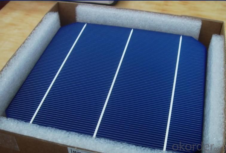
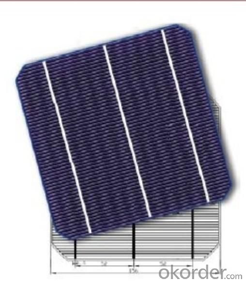
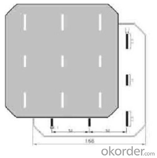
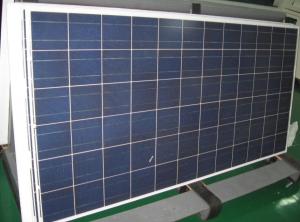
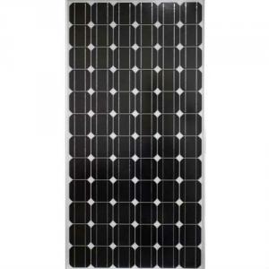
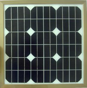
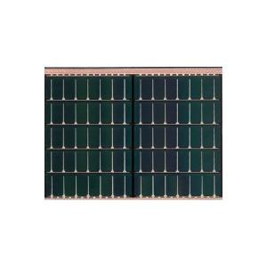
Details Of Mono Solar Cell 156mm
Specifications Of Mono Solar Cell 156mm
1.Mechanical data and design
Format | 156 mm × 156 mm ± 0.5 mm |
Thickness | - 210 μm ± 40 μm |
Front(-) | 1.5 mm bus bars (silver),blue anti-reflection coating (silicon nitride) |
Back (+) | 2.5 mm wide soldering pads (silver) back surface field (aluminium) |
2.Temperature Coefficient of Cells
Voc. Temp . coef.%/K | -0.35%/K |
Isc . Temp . coef.%/K | +0.024%/K |
Pm. Temp. coef.%/K | -0.47%/K |
3.Electrical Characteristic
Efficiency (%) | Pmpp (W) | Umpp (V) | Impp (A) | Uoc (V) | Isc (A) | FF (%) |
18.35 | 4.384 | 0.526 | 8.333 | 0.63 | 8.877 | 78.3% |
18.20 | 4.349 | 0.526 | 8.263 | 0.63 | 8.789 | 78.54% |
18.05 | 4.313 | 0.525 | 8.216 | 0.63 | 8.741 | 78.32% |
17.90 | 4.277 | 0.524 | 8.161 | 0.629 | 8.713 | 78.04% |
17.75 | 4.241 | 0.523 | 8.116 | 0.629 | 8.678 | 77.70% |
17.60 | 4.206 | 0.521 | 8.073 | 0.628 | 8.657 | 77.36% |
17.45 | 4.170 | 0.519 | 8.039 | 0.628 | 8.633 | 76.92% |
17.30 | 4.134 | 0.517 | 8.004 | 0.626 | 8.622 | 76.59% |
17.15 | 4.098 | 0.516 | 7.938 | 0.625 | 8.537 | 76.80% |
17.00 | 4.062 | 0.512 | 7.933 | 0.625 | 8.531 | 76.18% |
16.75 | 4.002 | 0.511 | 7.828 | 0.625 | 8.499 | 75.34% |
16.50 | 3.943 | 0.510 | 7.828 | 0.625 | 8.484 | 74.36% |
4.Intensity Dependence
Intensity [W/m2] | Isc× [mA] | Voc× [mV] |
1000 | 1.00 | 1.000 |
900 | 0.90 | 0.989 |
500 | 0.50 | 0.963 |
300 | 0.30 | 0.939 |
200 | 0.20 | 0.920 |
Advantage Of Mono Solar Cell 156mm
1: high quality cell, Level A cell
2: Dimensione:125*125mm Diagonal:150mm / 165mm
Dimensione:156*156mm Diagonal:200mm
3: Qualified certification: TUV,CE certification.
4: Warranty: five years for whole unit
Usage/Application Of Mono Solar Cell 156mm
Monocrystalline solar cells are currently the fastest developing a solar cell, its structure and production process has been finalized, the products have been widely used for space and ground. Such solar cells with high purity silicon rods as raw materials. Silicon rods, material performance indicators in order to reduce production costs, and now solar terrestrial applications such as the use of solar grade somewhat relaxed. Some semiconductor devices can also be used for processing materials and discard the head and tail of silicon materials, solar cells after re-drawn into a dedicated silicon rods.
Packaging & Delivery Of Mono Solar Cell 156mm | |
Packaging Detai | Packaging Detail:Export Carton and Pallet or under customer request. |
Delivery Detail:10-20days | |


New Discovery of Solar Energy Material and Solar Cells
Nature prefers crystals. Salt, snowflakes, and quartz crystals are three typical examples, which is characterized by atoms and molecules are arranged in a unique lattice.
Industry also loves crystals. Electronic components is a crystal family, also known as semiconductors, the most famous is the silicon material.
In order to make semiconductor practical engineer must adjust its crystalline arrangement to control the start and stop the flow of electrons. Semiconducto r engineers need to know precisely the lattice energy of electrons required to move this energy value is called the energy gap. Similar to silicon, gallium arsenide and germanium and other semiconductor materials, they each have a unique energy gap of the crystal lattice. Through the determination of the energy gap, can determine what kind of material is suitable for electronic functions.
An interdisciplinary research team at Stanford University has successfully produced a semiconductor crystal with a variable energy gap. Such a semiconductor may be used as a solar cell, which is very sensitive to certain spectrum, from the sun to absorb more energy.
This raw material itself is not something new. Molybdenum disulfide (MoS2) is a crystalline rock, such as quartz, as a catalyst can be used to refine and lubricants.
Molybdenum disulfide is a single-layer structure: a triangular lattice of molybdenum atoms joins two sulfur. The nature of the rock is made up of many such single layer of material laminated together. Each has a single layer of molybdenum disulfide semiconductor potential applications.
Use of such a semiconductor material, we can get a great energy gap. This will have a beneficial aspect of the sensor, solar and other electronic applications.
Scientists have graphene endless praise. It found that graphene materials won the Nobel Prize, which is a single-layer structure consisting of a single layer of carbon atoms flat pendulum.
In 2012, the nuclear industry and MIT materials scientist devised a theory relates to semiconductor applications molybdenum disulfide monolayer. For any semiconductor, engineers must change its lattice arrangement so as to control the flow of electrons. For silicon, this adjustment comprises mixing a small amount of chemical substances in the crystal lattice.
Its scalability in the process is the most exciting thing. At the same time, from an industrial point of view, molybdenum disulfide very cheap.